Call Us +91-8735997171
Office
E-223, Electronics Estate, G.I.D.C. Sector-26, Gandhinagar-382 028, Gujarat - India
Call Us +91-8735997171
Office
E-223, Electronics Estate, G.I.D.C. Sector-26, Gandhinagar-382 028, Gujarat - India
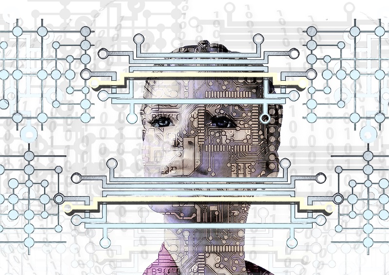
PCB reverse engineering (also known as reverse technology) is a process of printed circuit board design technology reproduction, reverse analysis and research of a target PCB board. It is also to deduce and obtain the design of the product's processing flow, structure, functional characteristics, and technical specification elements to produce products with similar, but not exactly the same, functions. Reverse engineering originates from hardware analysis in the commercial and military fields. Its primary purpose is to directly analyze the finished product and push out its design principle when the necessary production information cannot be easily obtained.